New Silicon Reach-Through Avalanche Photodiodes
Photodiodes with Enhanced Sensitivity in the DUV/UV Wavelength Range
Abstract - Many applications, particularly in the medical and bio-medical fields, require highly sensitive detectors in the short wavelength range (blue and below); so far there have been few commercially available avalanche photodetectors with adequate performance to satisfy demands of such applications. We have developed a new silicon reach-through avalanche photodiode (RAPD) operating in the blue wavelength range with improved sensitivity and noise performance superior to any similar detectors available on the market today. This has been accomplished thanks to an innovative, ultra-thin and highly doped surface top layer grown using a new epitaxial technique developed at Delft University of Technology in The Netherlands. An important additional advantage of this new RAPD is its unmatched noise performance over the widest commercially available wavelength range from 250 nm to 1100 nm. Short wavelength response is limited only by the transmission of the package window optimized for wavelengths starting at 250 nm and up, but devices can operate at wavelength even below 100 nm if assembled in a vacuum.
INTRODUCTION
Beyond Borders
Silicon reach-through avalanche photodiodes (RAPD) are types of avalanche photodiodes (APD) made on high quality, float zone, 5000 ohm-cm silicon material as opposed to regular APDs made on epitaxial silicon wafers and as such have inferior performance to the RAPD. Silicon RAPD is highly sensitive photo detector used in low background applications requiring low noise and high bandwidth sensors. Operating in the avalanche mode, the RAPD devices generate a cascade of moving carrier pairs for each absorbed photon, creating measurable signal current even when extremely weak photon fluxes are present [1]. The avalanche multiplication process is based on carrier multiplication in a strong electric field region. Carriers acquire sufficient energy between collisions to eject valence electrons from the lattice, and in that way create multiple electron-hole pairs.
The efficiency of new carriers’ generation is governed by ionization coefficients of both carriers and is a strong function of the electric field and temperature. Theoretical considerations of the process are complicated, but extensive studies done over the years [2] have provided comprehensive insight into how the devices operate and allow for selection of the optimum configuration needed for each different application. In this paper we will describe how an already wide sensitivity range of silicon RAPD devices is being extended deep into the shorter wavelengths i.e. blue to deep ultra violet (DUV). This was accomplished by applying a novel thin film growth technique. The thin and highly doped layer produced with this deposition technique minimizes short wavelengths’ surface absorption loses thus significantly improving device sensitivity range for wavelengths less than 400 nm. This improvement has been sought for a long time, but latest advances in the bio-medical field have made the need for such high performance sensors even more urgent.
GENERAL DESCRIPTION
Beyond Borders
Silicon RAPD Structure
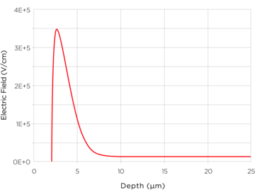
The silicon RAPD structure described in this paper is a p+ - π – p - n+ type [3]. In addition to highly doped contact layers on both sides of the structure, it consists of a narrow high-field region where the multiplication takes place and a much wider low-field region in which the incoming photons are absorbed. The design, impurity concentration, and electric field profiles are shown in Fig. 1.
Multiplication Gain
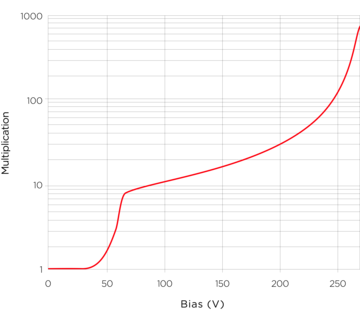
Impurity profiles, p-type first and n-type later, are adjusted so that when the depletion edge, driven by an external bias, reaches the high resistivity π; region, the peak electric field at the internal p-n junction is set to be just slightly below that required to initiate the avalanche breakdown. The depletion layer spreads rapidly out to the p+ contact when the external bias is incrementally increased beyond the point described in the previous sentence. However, the electric field throughout the device increases only slowly due to significant and fast increase in the depletion layer width. This results in a gradual shape of the multiplication characteristic shown in Fig. 2. To have the device operating in the linear mode the operating voltage range is limited by the requirement for avoidance of the avalanche breakdown. At the point of the avalanche breakdown the multiplication gain is infinite, resulting in an improper operation of the device. The proper linear mode operation of the device requires large, but finite multiplication gain. The operating voltages of the typical devices are in the 200 V to 400 V range, because carrier multiplication and photon absorption regions are geometrically separated as shown in Fig. 1. An impractical voltage well in excess of 1000 V would have to be used if two regions were combined into a single region. The separation of the multiplication and absorption regions results in a complex electric filed profile with the device noise performance depending significantly on the structure and impurity profiles.
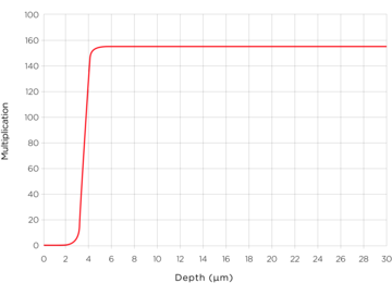
Both signal and noise considerations demand that the multiplication process is initiated by carriers having a higher ionization coefficient. Electrons are higher ionization coefficient carriers in silicon and for that reason RAPDs are designed so that the light enters at the p+ region surface. Under normal operating conditions both π and p regions are fully depleted, allowing for efficient collection of photo-generated electron-hole pairs. Photons have been absorbed in the π region and then separated by that region’s electric field, which is approximately 3x10⁴ V/cm. The electrons are subsequently swept into the π region where the electric field is sufficiently high to cause multiplication by impact ionization. Figure 3. shows a positional dependence of the electrons multiplication gain in an RAPD structure. The characteristic is a result of calculations using a one dimensional model implemented in a spreadsheet macro program [4]. The generated holes in the π region are on the other hand swept toward the p+ layer. They do not experience any gain and constitute a very small component of the overall hole current. The hole current consists mostly of the holes created by impact ionization in the multiplication region. The response time of silicon RAPD is determined primarily by the hole transit time and ranges from 400 psec to 5 nsec, depending on the width of the absorption layer. The situation when light is entering on the n+ layer side is possible as well, such as in the case of epitaxial APDs, but those devices are noisier and are used in less demanding applications.




Noise
Theoretical noise studies demonstrated that the noise component associated with the avalanche mechanism in the silicon RAPD devices is lower if only electrons are being multiplied. The Excess Noise Factor, F, quantifies the above effect as described below.
The noise density, in2, in an RAPD is given by the following equation [5]:
in2 = 2q (Is + (Idm+Ibk ) M2F)
- Is - Surface component of the dark current, which does not get multiplied,
- Idm - Bulk component of the dark current undergoing multiplication,
- Ibk - Background generated current,
- M – Multiplication gain,
- F – Excess Noise Factor.
The Excess Noise Factor, F, is given by [3]:
F = keffM + (1 – keff)(2 – 1/M)
- keff – the effective ratio of the hole to electron ionization coefficients.
The noise density is reduced by lowering the value of the Excess Noise Factor as shown by (1). keff is the primary quantity affecting the value of the Excess Noise Factor. Its value is always less than one, because the hole ionization coefficient is always smaller than the electron ionization coefficient in silicon. For multiplication gains higher than 10 and keff less than 0.1, (2) can be simplified to F = 2 + keffM. Consequently, low keff is highly desirable in order to achieve a low noise RAPD operation. In practical terms it means that RAPDs with lower value of keff will be able to operate at higher gains with a lower noise level.

Quantum Efficiency
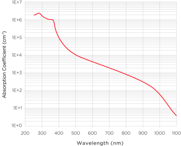
Light absorption in the silicon RAPD is governed by the silicon absorption coefficient shown in Fig. 4 [6]. Quantum efficiency is a fraction of the incident photon flux, which generates electron-hole pairs in the absorption region and contributes to the signal current
Quantum efficiency, η is given by [4]:
where r1 is the reflectivity of the front surface; r2 is the reflectivity of the back; d is the effective thickness of the light entry “dead” layer; w is the effective thickness of the absorption layer; and α is the absorption coefficient of silicon in the wavelength range of interest. The light entry “dead” layer is the p+ layer. The carriers generated in the layer do not participate in the multiplication process and thus do not contribute to the operation of the device. In order to maximize η, r1 should be made as small as possible by using an anti-reflecting coating, αw should be greater than unity, αd should be much less than unity, and r2 should be as close to one as possible.
For wavelengths below 800 nm (3) takes form:
η = (1-r1)exp(-αd)
Equation (4) shows that the contact layer on the light entrance side is critical and has to be as thin as practically possible if an increase in the sensitivity at short wavelengths is desired.
SPECTRAL COVERAGE IMPROVEMENTS
Beyond Borders
Based on the RAPD quantum efficiency discussion it is clear that thickness of the “dead” layer on the side where light enters the structure should be minimized to improve the short wavelength response of the device, but it has been difficult to accomplish such a thin and highly doped layer using standard processes common in today’s semiconductor wafer fabrication. The silicon absorption depth in the wavelength range of interest is shown in Fig. 5 where the shortest ‘1/e’ penetration depth is around 5 nm, implying that if the “dead” layer in our RAPD were 5 nm thick we would expect a 40% quantum efficiency at 250 nm. The absorption depth at the longer wavelengths is much longer making the RAPD operation far less sensitive to the thickness of the “dead” layer at those long wavelengths.
Since the p+ layer is the contact as well as the surface passivation layer, it has to be as highly doped as possible to prevent the internal electric field from reaching the surface of device and minimizing the series resistance of the layer. The problem is that the p+ layer is also the top layer on the surface where light enters the device and therefore it has to be as thin as possible. Those two opposite requirements have been difficult to reconcile up until now, because the high dopant solubility in silicon needed to achieve high surface concentrations is possible only at high temperatures, making sufficiently shallow layers created by diffusion, implantation or standard high temperature epitaxy impossible to produce. Fortunately, a novel epitaxial technique developed by the Silicon Device Integration Group at Delft University of Technology [8] provides the means of growing such thin and highly doped layers at lower temperatures, between 500 and 700 oC, while still achieving surface doping levels exceeding 1020 cm-3. With the help from the Silicon Device Integration Group, their innovative fabrication technique has been successfully incorporated in our RAPD processing sequence, yielding the devices described in this paper.
The deposition of the highly doped and thin p+ layer was performed in an ASM Epsilon One reactor using diborane B2H6 and hydrogen H2 as the gas source and carrier gas, respectively. The target layer thickness has been set to 3 nm. The layer deposition rate has been calibrated using variable angle ellipsometry measurements and confirmed by a Transmission Electron Microscope (TEM).
Once wafer processing has been completed, the devices were mounted onto TO-18 header and closed in a hermetically sealed package with the cap window made from the fused quartz with a special antireflective coating optimized for the wavelength range from 255 to 700 nm.
SUR500S8, which is Laser Components DG, Inc. (LCDG) product designation for this new silicon RAPD, has current-voltage (I-V), noise and spectral characteristics measured using setup depicted in Fig. 8. SUR500S8 will be used from now on as the designation for the new silicon RAPD device.


The light delivery part of the measurement setup consists of the Spectral Products ASBN Series deuterium/halogen light source combined with the Spectral Products CM110 1/8m monochromator and a grating optimized for the wavelengths range of interest. It delivers the light to a device under test (DUT) using a 600 μm core quartz fiber and special optics. The upper part of the setup including the Keithley 237 High Voltage SMU is used in DC measurements of the current flowing inside the device under dark and illuminated conditions. During those measurements the chopper is disabled and it is not obstructing the light path. Typical I-V characteristics obtained in such measurements are shown in Fig. 9, where the I-V characteristic measured under illumination shows the typical reach-through step seen also in the multiplication characteristic. The gradual increase of the current with the bias for the I-V curve measured under illuminations closely corresponds to the gradual increase of the multiplication gain shown in Fig. 2.
Spectral and noise characteristics of the device are measured using the instruments depicted in the lower section of the setup. The light output from the monochromator is chopped at 800 Hz and SUR500S8 is biased by the Keithley 6487 Picoameter/Voltage Source to operate at a multiplication gain close to 100. The signal from the SUR500S8 was conditioned by the transimpedance amplifier and monitored by the HP 3561A Dynamic Spectrum Analyzer. The short wavelength region i.e. up to 400 nm of the spectral characteristic is measured using the deuterium light source and the monochromator with the grating optimized for that wavelength range. The remainder of the characteristic, i.e. from 400 nm up, utilized the halogen light source and an appropriate grating optimized for that wavelength range. A calibrated OL 730-5EC UV-enhanced silicon reference detector from Gooch & Housego was used to measure optical power from the monochromator.
Measurement results, where the new SUR500S8 device is compared with the LCDG standard RAPD device, SAR500S3. It has to be emphasized that the SAR500S3 device was assembled using the same fused quartz cap as the SUR500S8 in order to keep the comparison meaningful.
Figure 10. Comparison of spectral characteristics of standard and new RAPD biased at M = 120
Significant improvements in the responsivity [9] at the shorter wavelengths i.e. below 400 nm are clearly visible in Fig. 10, but are even more evident when changes in quantum efficiencies of both devices are compared in Fig. 11. A SUR500S8 responsivity characteristic is also shown in Fig. 11 to demonstrate the responsivity level attainable by such devices for very short wavelengths. This is an important consideration because in bio-medical applications the signal levels are so low that it is practically impossible to detect a signal unless the device responsivity at the

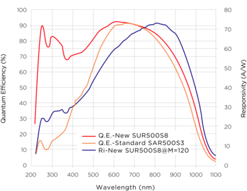
Figure 11. SUR500S8 quantum efficiency improvements
wavelengths is high. Another important consideration is minimizing the noise density at the bias levels of interest. Measurements of the responsivity at 400 nm and the noise density as a function of the bias performed on the new silicon RAPD are shown in Fig. 12. The noise density is bias independent in a wide range and up to the responsivity of about 50 A/W,
indicating that the low noise device operation is possible while at the same time achieving high responsivity levels. The optimum bias voltage is the voltage at which noise starts to increase more rapidly than the signal itself.

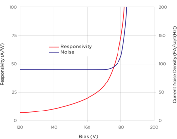
Figure 12. SUR500S8 responsivity at 400 nm and dark noise characteristics
However, it is difficult to see from Fig. 12 what that optimum operating bias would be because responsivity and noise density are changing very rapidly. The Noise Equivalent Power (NEP) [10] graph of the device as a function of bias shown in Fig. 13 is a better representation of the device performance and it clearly shows the optimum bias of the device.

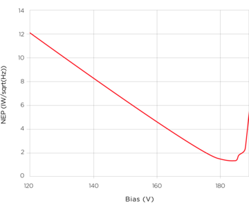
Figure 13. SUR500S8 Noise Equivalent Power
Based on the above noise measurements, it appears that the SUR500S8 can be operated at the
responsivity higher than 100 A/W at 400 nm. However, measurements described in this paper
were done having no background light, while in actual applications there always will be some
background, which will increase the level of noise in the device and shift the NEP characteristic
up and to the left. The NEP characteristic shift lowers the optimum responsivity of the device over
the complete wavelengths range. Since different applications have different background light levels
it is hard to predict what would be the optimum operating point for each individual case. For that
reason, each receiver is optimized in such a way that the SUR500S8 bias is adjusted under operating
conditions for each application so that its noise is equal to the noise of the preamplifier.
CONCLUSION
Beyond Borders
Using an innovative semiconductor processing technique, a new class of silicon RAPD devices has been produced that extends its usable operating range deep into the UV wavelengths in order to meet increasing demands for such devices in bio-medical applications. This has been accomplished thanks to an innovative, ultra thin and highly doped surface top layer, grown using a new epitaxial technique developed at Delft University of Technology in The Netherlands. In principle, the new silicon RAPD could operate very well even at wavelengths below 100 nm in a vacuum. Assembled into a typical TO package, the new silicon RAPD can operate at low noise levels at the responsivity in excess of 50 A/W with quantum efficiency peaking as high as 90% in the wavelength range between 255 nm and 400 nm.
ACKNOWLEDGMENT
D. Grubišić wants to express gratitude and appreciation to the Silicon Device Integration Group at Delft University of Technology, Prof. Nanver and T.L.M. Scholtes in particular, for their help and support on this project. The authors would like
to thank Diana Convay and Karl Weiss of Arizona State University LeRoy Eyring Center for Solid State Science for their help with ellipsometry and TEM characterizations. D. Grubišić would also like to thank Dr. Davorin Babić for helpful and insightful conversations during the paper preparation.
REFERENCES
[1] W.T. Tsang (Ed.), “Lightwave Communications Technology, Part D Photodetectors”, Semiconductors and Semimetals, Volume 22, Academic Press Inc., 1985.
[2] P.P. Webb, R.J. McIntyre, and J. Conrady, “Properties of avalanche photodiodes,” RCA Review, Vol 35, June 1974.
[3] Laser Components GmbH, “Silicon avalanche photodiodes”, Application Manual, http://www.lasercomponents.com/fileadmin/user_upload/ home/Datasheets/lc/applikationsreport/si-apds.pdf , (February 1, 2013)
[4] P.P. Webb, Private Communications, May 4, 2004.
[5] R.J. McIntyre, “Multiplication noise in uniform avalanche photodiodes,” IEEE Trans. On Electron Devices, Vol. ED 13, January 1966.
[6] M.A. Green and M. Keevers, "Optical properties of intrinsic silicon at 300 K," Progress in Photovoltaics, p. 189-192, 1995.
[7] E.D. Palik (Ed.), “Handbook of Optical Constants of Solids”, Academic Press Inc., Orlando, Florida, 1985.
[8] F. Sarubbi, T.L.M. Scholtes, and L.K. Nanver, “Chemical Vapor deposition of a-boron layers on silicon for controlled nanometer-deep p⁺n junction formation”, J. Electron. Mater., vol. 39, p. 162-173, 2010.
[9] R.D. Hudson, Jr., “Infrared System Engineering”, John Wiley & Sons Inc., 1969.
[10] S.M. Sze, “Physics of Semiconductor Devices”, Second Edition, John Wiley & Sons Inc., 1981.
Download
Beyond Borders
LASER COMPONENTS USA - Your competent partner for optical and optoelectronic components in the United States.
Welcome to LASER COMPONENTS USA, Inc., your expert for photonics components. Each product in our wide range of detectors, laser diodes, laser modules, optics, and more is worth every Dollar ($/USD). Our customized solutions cover all conceivable areas of application: from sensor technology to medical technology. You can reach us here:
116 South River Road
Building C
Bedford, NH 03110
USA
Phone: +1 603 821 7040
Email: info(at)

