Silicon Avalanche Photodiodes
Silicon Avalanche Photodiodes
Introduction
Beyond Borders


The purpose of this technical applications note is to provide the reader with a general background on multiplication processes in Silicon, and to describe some of the characteristics of silicon which make it such a useful material for the fabrication of PIN and Avalanche Photodiodes for visible and near IR applications. The paper will describe approaches to the design of APDs, and will provide other information that will be helpful to a potential user of APDs. Finally, a bibliography of a number of useful papers is provided, as a source of further information on subjects that may be treated only briefly in this paper.
Avalanche Multiplication Processes In Silicon
Beyond Borders
There is no intention to deal extensively with the subject of multiplication in silicon, since the mathematics involved is beyond the scope of this paper. For more information on this subject, the reader is referred to the first two references, and in particular to reference 1) entitled “Properties of Avalanche Photodiodes”, by P. P. Webb, R. J. McIntyre and J. Conradi; RCA Review, Vol. 35; June 1974.
However, in understanding the discussion of the following sections, it is useful to take a look at the multiplication process, and a number of characteristics of silicon that are so important for the fabrication of a multiplying device. In particular, it is important to know that – in general – electrons are much more ionizing than holes in silicon 4,5, so that in any useful APD design, electrons - rather than holes - should be swept by the electric field into the high field region where the multiplication takes place. Thus, there should be a p-type absorbing region of suitable width to absorb the incident radiation and that, as much as possible, the radiation should be able to enter this region without severe loss in any layer which is either n-type (e.g. through the junction in an n-p design), or in which the carrier lifetime is extremely short (e.g. a thick, heavily-doped p+ region). In either case the region would be essentially “dead”, and would absorb carriers that would contribute little or nothing to the multi-plied signal of the APD.
Quantum Efficiency
Beyond Borders


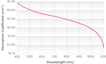
Figure 1: Absorption Coefficients in Silicon
In particular, at 1064 nm, good quantum efficiency can only be achieved with active layers that are at least several hundred micrometers. For a device in which the full thickness of the detector chip is active and is fully depleted by the applied bias voltage, except for narrow “dead” regions on either surface, the quantum efficiency, h, can be determined from the following formula:
Where: r1 is the reflectivity at the front surface, r2 is the reflectivity at the back surface, d is the effective thickness of the front “dead” layer, w is the thickness of the active layer, and α is the absorption coefficient of the radiation at the wavelength of interest.
From this, it is seen that for short wavelengths, (less than about 800 nm), where α is large, the 2nd and 3rd terms of the numerator, and the denominator all become unity, so that the expression reduces to:
η = [1– r1] exp (–d) (2)
However, at longer wavelengths such as, for example, 1064 nm, the reflection at the back surface becomes important in achieving high quantum efficiency. With a low value of r1 and a highly reflecting back surface, and the value of “d” small (less than about 1 µm at 1064 nm), equation (1) becomes, approximately:
η = [1– r1] [1– exp (–w)] [1+r2 exp(–
w)] (3)
Silicon Reach-Through APD
Beyond Borders
DESIGN:
The basic design of a reach-through avalanche photodiode consists of a narrow high-field region where the multiplication takes place, with a much wider low field region in which the incoming radiation is absorbed. The design, impurity concentration, and electric field profiles are shown in figure 2.
Figure 2: Silicon Reach-Through APD Structure, Concentration and Field Profiles


For satisfactory operation of the APD design of figure 2(a), the high resistivity p-type substrate must be fully depleted by the applied bias voltage. Generally, this works well provided the substrate wafer is not too thick, and required response times are not less than about 10 ns or so. However, fabrication of APDs on 4-inch wafers, as is now usually the case, will often mean that the substrate is thick, operating voltages are high, and response times slow. These problems can be avoided with the use of an epitaxial version of the design of figure 2. In this approach, a high-resistivity p-type layer is grown epitaxially on top of a low resistivity p-type substrate. The substrate may be any thickness, and its resistivity is chosen to be low enough that it does not introduce a significant series resistance. The thickness of the p-type epitaxial layer is typically chosen to be in the range 30 to 50 um, but may be narrower or wider, depending on the requirement of the application. A reach-through structure is achieved by introducing n- and p-layers, as shown in figure 2(a). When bias voltage is applied, the depletion layer stops at the interface between the substrate and the epitaxial layer. Where fast response is a requirement, the narrow active region of this version of the reach-through APD is normally the best option.
The main advantage of the reach-through design is that an APD with moderately wide absorbing region - e.g. up to several hundred micrometers – can be made which operates perfectly satisfactorily at a few hundred volts bias voltage, whereas the same device without the narrow high field region would require a much higher voltage which, for an APD with a thick active region, would be well in excess of 1000 volts.
One of the main disadvantages of the design is that (often) the APD cannot be operated at low gains, since the device will not operate at voltages below the reach-through voltage, and the gain at that point is usually greater than 1, and often as high as 10 or more.
Dead Layers
Finite “dead” layers will occur for light entering on either the junction or p+ surface of the APD of figure 2. For light incident on the p+ surface the “dead” layer is typically about 50% of the depth of that layer, when that layer has been diffused from a high concentration source. For relatively shallow diffusions, effective dead layers as thin as 0.1 to 0.2 µm can easily be achieved. For light entering the active region through the junction, the situation is somewhat more complex, since light incident on the n+ surface will result in holes being swept to the multiplying region. We have already noted in previous discussion that ionization coefficients for holes tend to be small, and therefore contribute relatively little to the multiplied signal. A full discussion of the issue is not presented here. However, in general, for light incident on the junction surface, the effective thickness of the “dead” layer is somewhat greater than the depth of the junction, and probably typically of the order of twice that depth. For very short wavelength illumination, the junction-surface “dead” layer can be very severe, even to the point of absorbing 100% of the radiation, whereas for long wavelength light, such as 1064 nm radiation, the effective “dead” layer thickness may be negligible.
Dark Current and Noise
In general, there are two main contributions to the dark current of an APD. The first of these is surface dark current, generated at or near the perimeter of the junction. This current occurs outside the multiplying region, and is therefore not multiplied. The second contribution to the dark current is bulk current, generated within the junction region, and in an APD this current component undergoes multiplication. Thus we have:
Id = Is + Idm M (4)
Where: Id is the total dark current, Is is the unmultiplied surface component of the dark current, Idm is the multiplied component of the dark current, and M is the Gain of the APD.
From the work of McIntyre1,2 it can be shown that the noise in a bandwidth of 1 hertz, in², in an APD is given by the following equation:
in2 = 2q [Is + (Idm + Ibk) M2F] (5)
Where: Ibk is the photo-induced background current in the multiplying region, and F is the excess noise factor, which for electrons entering the multiplying region is given by:
F = keff M + (1– keff) (2–1/M) (6)
Where: keff is the effective ratio of the hole to electron ionization coefficients.
Excess Noise Factor
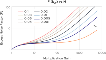
It is worthwhile to take a more careful look at the parameter keff, the effective ratio of the ionization coefficients in the APD. For gains greater than about 10, and low values of keff (less than about 0.1), equation (6) can be simplified to: F = 2 + keffM. From this we see immediately that a low value of keff is highly desirable in achieving low noise in the avalanche photodiode, and by extension, good signal-to-noise in a detection system in which an APD is the detector. In figure 3, the excess noise factor, F, for a number of different values of the parameter keff is plotted as a function of gain.


Figure 3: Excess Noise Factor in an APD as a function of keff and Gain
The ionization coefficient of holes is generally much less than that of electrons. However, in the design of an APD it is important to know that the effective ratio of the ionization coefficients (keff) is a function of the electric field in the multiplying region, having lower values for low fields, and higher values for high fields. Ideally, therefore, one would design an APD in which the electric field in the multiplying region is as low as possible. This is not always practical, however, since the width of the multiplying region, and therefore the reach-through voltage, is higher for low multiplying fields, and conversely, lower for high multiplying fields. Empirically, it is found that in a diffused version of a reach-through APD, a relationship exists between the reach-through voltage, VRT, and keff, which can be represented, approximately, by the following expression:
VRT = [16/keff ]0.7 35 < VRT < 200 (7)
For applications requiring relatively low operating voltage, such as a low cost APD for rangefinding applications, a reach-through voltage not higher than about 50 volts might be desirable, for which the k-factor would be of the order of 0.06. On the other hand, for a low light level application, it is desirable to have a very low value of keff, in order to achieve good signal-to-noise performance. For this type of application, the operating voltage of the APD can probably be as high as several hundred volts. Choosing, for example, a k-factor of about 0.02, the reach-through voltage would be of the order of 110 volts.
The field profile in the multiplying region, and therefore the k-factor, is critically dependent on the design of the avalanche photodiode, and computer modeling is necessary to predict the characteristics of a device when new fabrication parameters are chosen.
Temperature Effects
Ionization coefficients in silicon are dependent on the operating temperature of the device. While no mathematical expression can be presented here to describe this effect, it is found that ionization coefficients increase with decreasing temperature, and conversely, decrease with increasing temperature. Experimentally, it is found – to a first approximation – that the variation in applied bias voltage required in a typical reach-through APD, in order to maintain constant gain, can be represented by the following equation:
V(T) = V(T0) + 0.022w [T - T0] (8)
Where: V(T0) is the voltage applied at temperature T0 to achieve the desired multiplication, V(T) is the voltage required at temperature T to achieve the same multiplication, and w is the thickness of the active region (depletion layer), in micrometers.
For example, if w is 100 µm, then the voltage adjustment required in order to maintain constant gain, is about 2.2 volts per ºC.
Capacitance
To a fairly good approximation, an avalanche photodiode can be thought of as a parallel plate capacitor, having an area equal to the total area of the junction, whether multiplying or not. The capacitance can be calculated from the following equation:
C = kε0 A/w (9)
Where: k is the dielectric constant (about 12 for silicon), ε0 is the permittivity of free space, A is the area of the device, and w is the thickness of the depletion layer.
Signal-To-Noise Ratio
Beyond Borders
The main factors determining the noise characteristics of an avalanche photodiode have been discussed previously in sections 4.3 and 4.4. In this section we combine that information with the noise characteristics of the amplifier to determine the signal-to-noise ratio as a function of the multiplication factor of the APD.
Making use of equation (5), and adding a term for the noise in the signal (assumed to be DC in this example), and another term for the amplifier noise (assuming a noiseless operational amplifier), we can describe the overall shot noise by the following simplified equation:
in2 = 2q [ Is + (Idm + Idcsig + Ibk) M2F ] B + 4kTB/Rf (10)
Where: Idcsig is the dc component of the signal Isig, B is the noise bandwidth of the system, k is Boltzmann’s constant, T is the temperature in ºK, and Rf is the feedback resistor. The excess noise factor, F, is as per equation (6).
From this, we can write an expression for the signal-to-noise ratio in the APD, with DC signal current Isig falling on the active region of the APD:
S/N = [ Isig2 M2 ] / {2q [Is + (Idm + Idcsig + Ibk) M2F ] B + 4kTB/Rf } (11)
We note in equation (11) that the factor M2 appears in both the numerator and the denominator, so that an increase in gain will increase the signal-to-noise ratio only if the term in which M²F appears is not already the dominant term in the denominator. In practical terms, high gain will improve the S/N ratio in detection systems where the excess noise factor F is small, and the three multiplied currents in the denominator are small, and/or the noise of the amplifier is high. Conversely, in a system having very low noise in the amplifier and/or high multiplied current in the APD (such as, for example, a high level of background power falling on the APD), the optimum gain is likely to be low, or even unity.


| Singnal power | lsig | 1E-09 | W |
| k-factor | keff | 0.01 | - |
| Wavelength | λ | 650 | nm |
| Q.E. | η | 69 | % |
| Background current | lbk | 0 | A |
| DC signal current | ldcsig | 3.6E-10 | A |
| Feedback resistor | Rf | 1E+05 | Ohms |
| Temperature | T | 298 | K |
| Bandwidth | B | 1E+04 | Hz |
| Mult. dark current | ldm | 1E-11 | A |
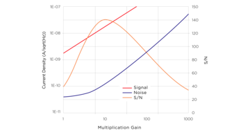
In figure 4, the S/N ratio is plotted for a particular low-level detection system in which the optimum gain is moderately high. The table shows the values of the parameters used in the calculation. For this calculation, a DC signal input was assumed, which results in a significant contribution to the noise from the signal itself. In many systems, the signal would be a pulse, or a series of pulses, for which the duty cycle would be low, resulting in a reduction in the noise, since only the DC component of the signal appears in the noise calculation.
In a final example, shown in figure 5, the S/N ratio has been plotted for a case where a high level of back-ground power is falling on the APD, (0.1 µW), which might be the case for an application such as a laser rangefinder, operating in daylight conditions. Even with the use of an optical filter to limit the background radiation to a small part of the spectrum on either side of the wavelength of the laser source, background power levels of this magnitude would not be unusual. The point of the example of this figure is to show that under certain conditions, the use of high gain in the APD will result in poorer S/N. In the example shown, the optimum gain for the APD in the system would be of the order of about 10.
Figure 5: S/N Calculation. High noise, Low Optimum Gain


| Singnal power | lsig | 1E-08 | W |
| k-factor | keff | 0.04 | - |
| Wavelength | λ | 1064 | nm |
| Q.E. | η | 20 | % |
| Background current | lbk | 1.7E-08 | A |
| DC signal current | ldcsig | 1.7E-09 | A |
| Feedback resistor | Rf | 1E+05 | Ohms |
| Temperature | T | 298 | K |
| Bandwidth | B | 1E+04 | Hz |
| Mult. dark current | ldm | 1E-11 | A |
References
Beyond Borders
1) “Properties of Avalanche Photodiodes”; P. P. Webb, R. J. McIntyre, and J. Conradi; RCA Review, Vol. 35, June 1974
2) “Multiplication Noise In Uniform Avalanche Diodes”; R. J. McIntyre; IEEE Trans. on Electron Devices, Vol. ED 13, January 1966
3) Temperature Effects in Silicon Avalanche Photodiodes; J. Conradi, Solid State Electronics, Vol. 17, Jan 1974
4) “Ionization Rates of Holes and Electrons in Silicon”; C. A. Lee et al; Phys. Rev., Vol. 134, May 1964
5) W. N. Grant; Solid State Electronics, Vol. 16, (1973)
LASER COMPONENTS UK - Your competent partner for optical and optoelectronic components in the United Kingdom.
Welcome to LASER COMPONENTS UK Ltd., your expert for photonics components. Each product in our wide range of detectors, laser diodes, laser modules, optics, fiber optics, and more is worth every Pound (£/GBP). Our customized solutions cover all conceivable areas of application: from sensor technology to medical technology. You can reach us here:
Goldlay House, 114 Parkway
Chelmsford Essex CM2 7PR
United Kingdom
Phone: +44 1245 491 499
Email: info(at)
