Avalanche Multiplication Process in Silicon
Silicon - Made for VIS to NIR Photodiodes
We will provide you with a general background on multiplication processes in Silicon, and describe some of the characteristics of silicon which make it such a useful material for the fabrication of PIN and Avalanche Photodiodes for visible and near IR applications.
We will describe approaches to the design of APDs, and will provide other information that will be helpful to a potential user of APDs. Finally, a bibliography of a number of useful papers is provided, as a source of further information on subjects that may be treated only briefly in this paper.
Avalanche Multiplication Processes In Silicon
There is no intention to deal extensively with the subject of multiplication in silicon, since the mathematics involved is beyond the scope of this paper*.
However, in understanding the discussion of the following sections, it is useful to take a look at the multiplication process, and a number of characteristics of silicon that are so important for the fabrication of a multiplying device. In particular, it is important to know that – in general – electrons are much more ionizing than holes in silicon 4,5, so that in any useful APD design, electrons - rather than holes - should be swept by the electric field into the high field region where the multiplication takes place.
Thus, there should be a p-type absorbing region of suitable width to absorb the incident radiation and that, as much as possible, the radiation should be able to enter this region without severe loss in any layer which is either n-type (e.g. through the junction in an n-p design), or in which the carrier lifetime is extremely short (e.g. a thick, heavily-doped p+ region). In either case the region would be essentially “dead”, and would absorb carriers that would contribute little or nothing to the multiplied signal of the APD.
*For more information on this subject, the reader is referred to the first two references, and in particular to reference 1) entitled “Properties of Avalanche Photodiodes”, by P. P. Webb, R. J. McIntyre and J. Conradi; RCA Review, Vol. 35; June 1974.
Quantum Efficiency
As noted in the previous paragraph, in designing or selecting an Avalanche Photodiode for a specific application, it is important to know certain characteristics of the silicon. In particular, knowledge of the absorption properties of silicon as a function of the wavelength of the incident radiation is necessary in order to determine the thickness of the active layer (i.e. the absorbing region) needed to obtain acceptable quantum efficiency.
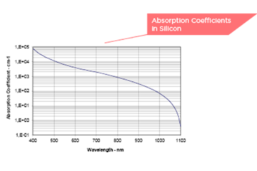
Figure 1 shows the absorption coefficient of silicon as a function of wavelength in the range 400 to 1100 nm.
From figure 1 we note that the absorption coefficient is very high for shorter wavelengths, meaning that good quantum efficiency can be achieved with relatively narrow active layers. On the other hand, the opposite is true for longer wavelengths.
In particular, at 1064 nm, good quantum efficiency can only be achieved with active layers that are at least several hundred micrometers. For a device in which the full thickness of the detector chip is active and is fully depleted by the applied bias voltage, except for narrow “dead” regions on either surface, the quantum
efficiency, h, can be determined from the following formula:
Where r1 is the reflectivity at the front surface, r2 is the reflectivity at the back surface, d is the effective thickness of the front “dead” layer, w is the thickness of the active layer, and a is the absorption coefficient of the radiation at the wavelength of interest.


Figure 1: Absorption Coefficients in Silicon
From this, it is seen that for short wavelengths, (less than about 800 nm), where a is large, the 2nd and 3rd terms of the numerator, and the denominator all become unity, so that the expression reduces to:
[2] h = [ 1 - r1] exp(-ad)]
However, at longer wavelengths such as, for example, 1064 nm, the reflection at the back surface becomes important in achieving high quantum efficiency. With a low value of r1 and a highly reflecting back surface, and the value of “d” small (less than about 1 µm at 1064 nm), equation [1] becomes, approximately:
[3] h = [1– r1] [1– exp (–aw)] [1+r2 exp(–aw)]
Beyond Borders
Silicon Reach-Through APD
Design
The basic design of a reach-through avalanche photodiode consists of a narrow high-field region where the multiplication takes place, with a much wider low field region in which the incoming radiation is absorbed. The design, impurity concentration, and electric field profiles are shown in figure 2.
Figure 2: Silicon Reach-Through APD Structure, Concentration, and Field Profiles
Request Form - Gated Content


LASER COMPONENTS Germany - Your competent partner for optical and optoelectronic components in Germany.
Welcome to LASER COMPONENTS Germany GmbH, your expert for photonics components. Each product in our wide range of detectors, laser diodes, laser modules, optics, fiber optics, and more is worth every Euro (€/EUR). Our customized solutions cover all conceivable areas of application: from sensor technology to medical technology. You can reach us here:
Werner-von-Siemens-Str. 15
82140 Olching
Deutschland
Phone: +49 8142 2864-0
Email: info(at)